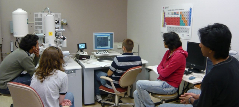
Description
The Hitachi S-4700 FE-SEM is a scanning electron microscope used for detailed image analysis of devices and circuits fabricated in the NanoFab. Under ideal conditions, it can magnify images up to 500 kX and can resolve features down to 2 nm. It also is equipped with an energy dispersive X-ray analysis tool to identify elemental materials. The specimen stage is capable of tilting up to 60 degrees with full 360 degrees in a continuous rotation. It can accommodate a sample up to 100 mm in diameter. The beam accelerating voltage is variable from 0.5–30 keV.
Benefits of Using the FE-SEM
Obtain high resolution imaging at low accelerating voltage.
With the tungsten emitter SEM, great skill is required to produce a high resolution image at low voltage. High resolution images, at high and low voltages, are easily produced with the S-4700 FE-SEM.
Accelerating voltage can be changed in smaller increments.
The kV can be changed by 1 kV increments on the FE-SEM, rather than in increments of 5 kV on the tungsten filament SEM. The lowest accelerating voltage the FE-SEM can achieve is 0.5 kV.
Have more control of working distance range.
Working distance can be changed in less than 1 mm increments, from 1 mm to 27 mm.
Windows based software makes operation easier because of its more user friendly interface.
Familiarity with Windows operating system software leads to greater productivity. Integrated column controls make switching between operating modes quick and easy. Fewer manual adjustments of the column are required.
