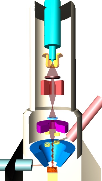
Signal Source and Detection
Creating a Circuit
Since the FE-SEM is in effect an electrical circuit, the specimen must be conductive. In the tungsten source SEM, any nonconductive specimen is coated with a very thin layer of conductive material in order to provide a pathway for the negatively charged electrons to escape the beam impact site. One critical advantage provided by FE-SEM imaging is a significant reduction in observed charging effects due to the low operating voltage capabilities of the instrument. When a coating is required, a platinum/palladium coating 5 nm thick is most commonly chosen. (Details of specimen coating is discussed in another section of this module.) This will prevent a charge from forming on the specimen. If charging does occur, image resolution is degraded and imaging can become impossible.
Types of Scattering
As the beam electrons interact with the specimen, they are scattered elastically (changing their trajectory but carrying almost the same kinetic energy) and inelastically (losing energy but remaining at almost the same trajectory). Most of the electrons are carried to the ground circuit, but some of them penetrate the sample and, after losing only a small amount of energy, escape the sample as backscatter electrons (BSE). The number of backscatter electrons produced in the beam impact site is a function of the elemental composition of the sample, and these electrons are collected to provide compositional information about the sample. During inelastic scattering, loosely bound electrons located on the outer shells are knocked out of the sample by the incident electrons. Called secondary electrons (SE), they are useful in imaging the surface topography.
Upper and Lower Detectors
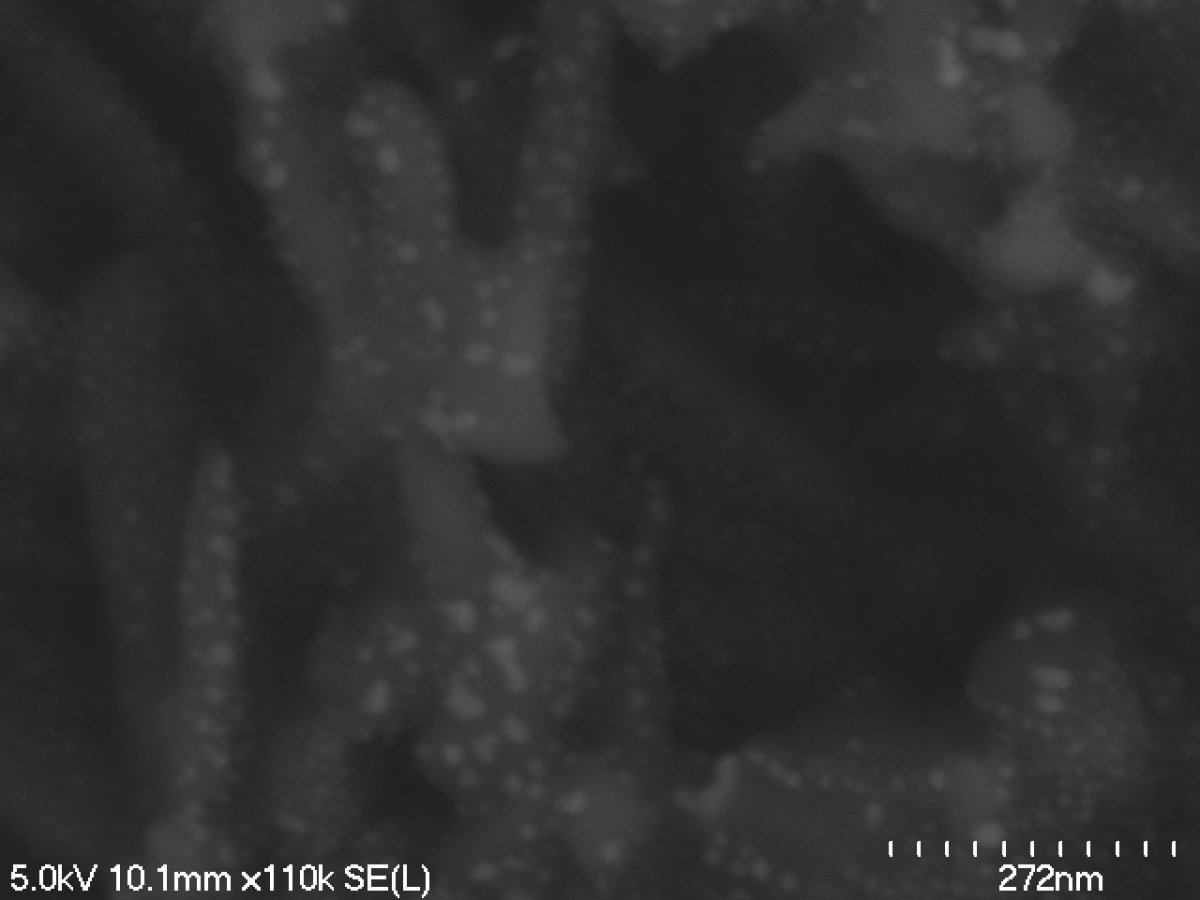
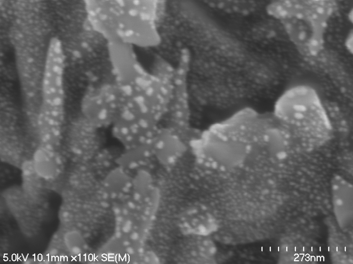
The signals produced during the electron beam-specimen interactions (SE, BSE, and X-rays) are sensed by detectors. The detectors are specifically designed to specialize in and detect one or more types of signals. The FE-SEM is equipped with two detectors. Both are of the Everhart-Thorley type used for electron imaging. One, called the lower detector, is positioned horizontally near the specimen. The lower detector collects all types of SE signals and some BSE signals. Because of its placement in the column, the lower detector can provide a good view of topographic detail. Also, using the combination of SE and BSE signals, there are fewer observed charging effects.
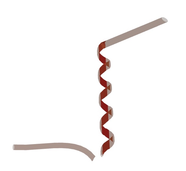
FE-SEM Electron Beam Path Animation
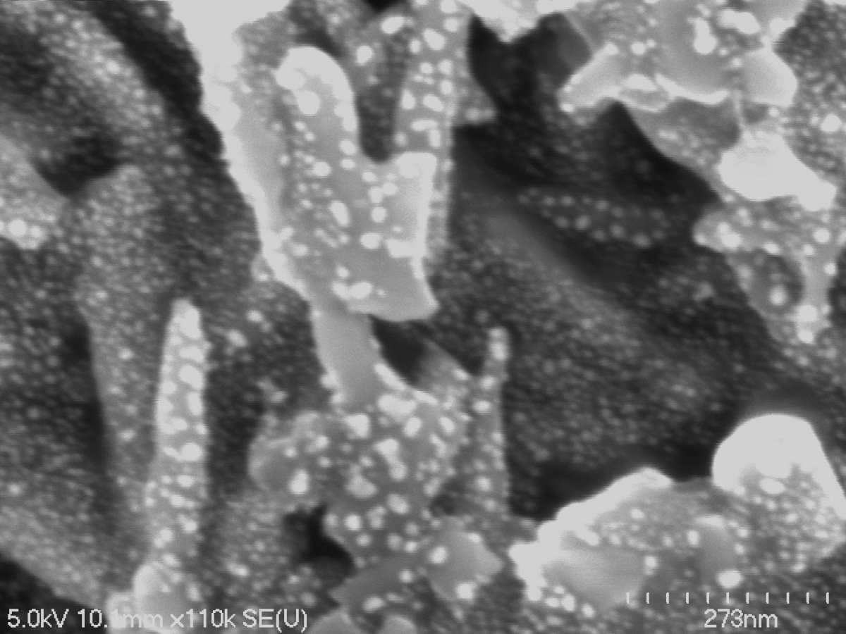
The upper detector is positioned above the specimen within the objective lens, operating through the lens collection. This type of collection seems counter-intuitive, because signal electrons must travel up the column at the same time the electron beam is moving down towards the specimen. The specimen itself is surrounded by a field causing the electrons to spiral upwards. Additionally, the objective lens is an inverted snorkel lens, creating an immersion lens field which also attracts the signal electrons. A special ExB filter prevents signal electrons from interfering with the beam, allowing for the detection of high resolution SE and BSE. This detector is preferred when using high magnifications and when high resolution imaging is required. The upper detector also has the ability to detect signals at all working distances and with all accelerating voltages, making it useful for a variety of functions. Either detector can be selected for imaging or both can be used in tandem.