
Michigan Tech’s new Scanning Transmission Electron Microscope lets researchers zoom in to understand the big picture at the atomic scale.
Housed in a specially constructed brick building at the south end of Michigan Technological University’s campus is the FEI 200kV Titan Themis Scanning Transmission Electron Microscope (S-TEM). One of only two Titans in the state of Michigan, the microscope is capable of imaging at the atomic scale, providing chemical information from a sample and can also operate as a transmission electron microscope.
Such a powerful tool is one of the newest in the Applied Chemical and Morphological Analysis Laboratory’s (ACMAL) arsenal.
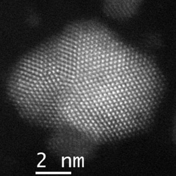
S-TEMs use an electron beam less than an angstrom wide (smaller than an atom) to create a digital image of an atom column, allowing researchers to see how atoms bond and the structure of a given sample. Stephen Hackney, professor of materials science, likened it to looking down a stack of transparent cannon balls—extremely tiny ones.
In numerous fields—materials science and engineering, chemistry, physics, geology, biomedical engineering, mechanical engineering and others—S-TEM provides a way to understand atomic-level interactions that effect materials, chemicals and other substances at a macro-scale. Analyzing S-TEM outputs means zooming in on the tiniest details to understand the big picture.

Facebook Live: Gaining Understanding on an Atomic Level
Live lab tour of the S-TEM facility at Michigan Tech.
An Entire World Under the Lens
A few of the current projects under the Titan lens at Michigan Tech include:
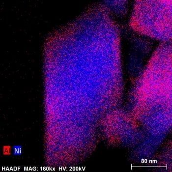
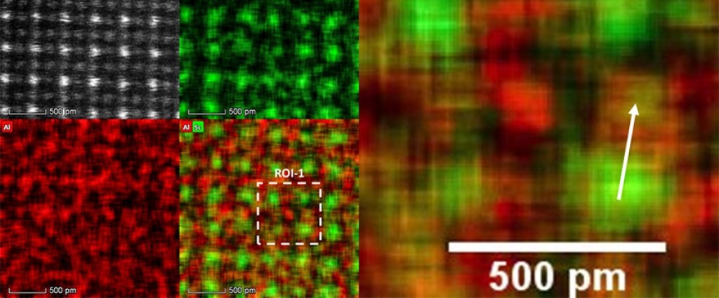
- Studying the microstructure of high-temperature aluminum alloys. Because of its light weight, aluminum offers possibilities to both the military and transportation sectors. Understanding how aluminum-alloy atoms behave under high temperatures helps scientists work with the material to strengthen it. Light-weight rockets take satellites into orbit more easily than heavy ones, after all.
- Building better batteries. Hackney is working with Duracell Batteries to improve the materials in its copper-top battery line so that the batteries last even longer. “[Duracell is] interested in the way they process the material – sometimes it comes out one way, and it works, and sometimes it comes out a different way and it doesn’t work,” Hackney says. “They want to know what happens at the atomic scale, why that makes it work in some cases but not in other cases.”
- John Jaszczak, professor of physics, and Christopher Stefano, associate curator at the A.E. Seaman Mineral Museum, seek to understand how certain minerals form over the eons—how the atoms have stuck together in interesting ways as proof of the eons of fabrication they went through. Understanding mineral structures gives researchers the ability to manufacture them synthetically, which can be useful for society (and not just rock lickers).
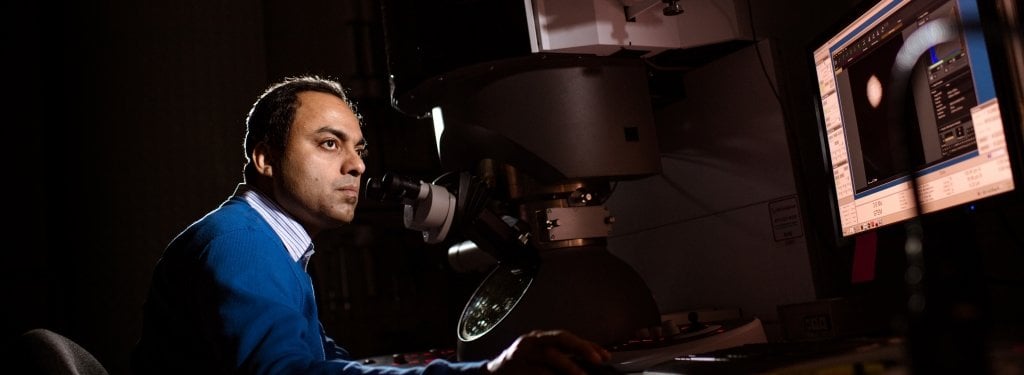
Pinaki Mukherjee was recently hired as the S-TEM specialist. He earned his doctorate from the University of Nebraska-Lincoln, where he first worked with transmission electron microscopes. He completed post-doctoral work at Rutgers University and is affiliated with the Lawrence Berkeley National Laboratory’s National Center for Electron Microscopy.
Mukherjee processes some samples and calibrates the microscope, which is extremely sensitive to temperature changes and vibrations, but also trains faculty and graduate students on how to operate the Titan. Though he can process samples more quickly than most, he’s aware of the microscope’s limitless potential.
The samples analyzed in the S-TEM must be extremely thin in order to form useful images from the transmitted electrons, which requires some expertise. Owen Mills, senior research engineer and scientist and director of ACMAL, is an expert in several types of sample preparation for polymers, bio-materials, ceramics and metals and assists most users in developing useful specimens.
Commenting on the extraordinarily small size of material examined in a typical experiment, Hackney says, “When I first arrived at Michigan Tech 30 years ago, Professor Tom Courtney pointed out that if you take all the material that’s been analyzed by transmission electron microscopy or S-TEM up 1985 and put it all together, you might make the head of a pin. However, now I think it is probably the whole pin.”
All the World’s a Stage
“Michigan Tech is known for being a hands-on school,” says Mills. “We want to train students to do the work themselves so they can go out and do the work in industry or at other academic institutions.”
A key function of the microscope is its ability to observe material behavior at atomic resolution while subjecting atoms to various stimuli. Samples can be placed on stages that elevate temperature, apply different voltages, deform materials by applying force, and allow examination of materials behavior in a liquid environment.
Another function of the microscope is creating three-dimensional models of materials using electron tomography to examine a sample from all angles.
The S-TEM facility is also open to researchers and scientists from other institutions. Visit the S-TEM facility website for more information about booking the lab for sample processing.
“It's really a tool that is only limited by the limits of our imaginations,” Mills says. “The microscope itself is a ticket into a new world. We’re really fortunate; there are very few of these microscopes around.”
Michigan Technological University is an R1 public research university founded in 1885 in Houghton, and is home to nearly 7,500 students from more than 60 countries around the world. Consistently ranked among the best universities in the country for return on investment, Michigan's flagship technological university offers more than 185 undergraduate and graduate degree programs in science, technology, engineering, mathematics, computing, forestry, business, health professions, robotics, psychology, social sciences, humanities, and the arts. The rural campus is situated just miles from Lake Superior in Michigan's Upper Peninsula, offering year-round opportunities for outdoor adventure.


Comments