Location
Michigan Tech Alumni Center 149
Contact
Cell: 906-299-2714
Access Type
Instrument Details
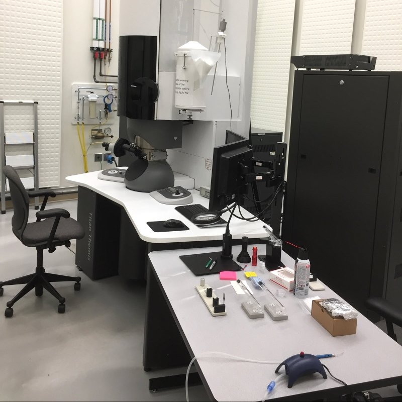
The FEI 200kV Titan Themis Scanning Transmission Electron Microscope (STEM) is a scanning transmission electron microscope with several key capabilities.
This microscope positions Michigan Tech faculty on the leading edge of new imaging capability for structural and chemical analysis at the nanoscale. The microscope is housed in a building specially constructed for such an instrument capable of atomic resolution. This instrument represents one of only two Titans found in higher education in the state of Michigan. The Themis has a full complement of state-of-the-art accessories, including specialized specimen holders that extend the STEM utility.
Capabilities
- Accelerating Voltages from 80–200 kV
- Probe corrector (Cs) enabling atomic resolution STEM imaging
- High-angle Annular Dark-Field (HAADF) detector
- Segmented Annular Dark-field (ADF) detectors
- ChemiSTEM Super X-ray Energy Dispersive Spectrometer (EDS)
- TEM / STEM Tomography analysis
- STEM EDS Tomography
- Gatan Image Filter Quantum enabling Electron Energy Loss Spectroscopy (EELS) and Energy Filtered TEM (EFTEM)
- Protochips Axon Synchronicity enabling vision learning based drift correction for all types of TEM holders, and full integration for in situ analysis with Protochips TEM holder
- TEM Sample Holders
- Single Tilt holder (FEI/ThermoFisher)
- Beryllium tip Double Tilt holder (FEI/ThermoFisher)
- Room temperature tomography holder (Fischione) for both TEM and STEM tomography
- Electrical bias and Heating stage NanoEx holder (FEI/ThermoFisher)
- STM Nanoindentation holder (Nanofactory)
- Double tilt electric bias holder (Nanofactory)
- Poseidon 510 liquid cell holder (Protochips)
Vendor
FEI / ThermoFisher Scientific