Beyond Silicon: Transistors without Semiconductors

For decades, electronic devices have been getting smaller, and smaller, and smaller. It’s now possible—even routine—to place millions of transistors on a single silicon chip.
But transistors based on semiconductors can only get so small. “At the rate the current technology is progressing, in 10 or 20 years, they won’t be able to get any smaller,” said physicist Yoke Khin Yap of Michigan Technological University. “Also, semiconductors have another disadvantage: they waste a lot of energy in the form of heat.”
Scientists have experimented with different materials and designs for transistors to address these issues, always using semiconductors like silicon. Back in 2007, Yap wanted to try something different that might open the door to a new age of electronics.
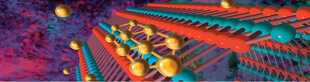
“The idea was to make a transistor using a nanoscale insulator with nanoscale metals on top,” he said. “In principle, you could get a piece of plastic and spread a handful of metal powders on top to make the devices, if you do it right. But we were trying to create it in nanoscale, so we chose a nanoscale insulator, boron nitride nanotubes, or BNNTs for the substrate.”
Yap’s team had figured out how to make virtual carpets of BNNTs,which happen to be insulators and thus highly resistant to electrical charge. Using lasers, the team then placed quantum dots (QDs) of gold as small as three nanometers across on the tops of the BNNTs, forming QDs-BNNTs. BNNTs are the perfect substrates for these quantum dots due to their small, controllable, and uniform diameters, as well as their insulating nature. BNNTs confine the size of the dots that can be deposited.
In collaboration with scientists at Oak Ridge National Laboratory (ORNL), they fired up electrodes on both ends of the QDs-BNNTs at room temperature, and something interesting happened. Electrons jumped very precisely from gold dot to gold dot, a phenomenon known as quantum tunneling.
“Imagine that the nanotubes are a river, with an electrode on each bank. Now imagine some very tiny stepping stones across the river,” said Yap. “The electrons hopped between the gold stepping stones. The stones are so small, you can only get one electron on the stone at a time. Every electron is passing the same way, so the device is always stable.”
Yap’s team had made a transistor without a semiconductor. When sufficient voltage was applied, it switched to a conducting state. When the voltage was low or turned off, it reverted to its natural state as an insulator.
Furthermore, there was no “leakage”: no electrons from the gold dots escaped into the insulating BNNTs, thus keeping the tunneling channel cool. In contrast, silicon is subject to leakage, which wastes energy in electronic devices and generates a lot of heat.
Other people have made transistors that exploit quantum tunneling, says Michigan Tech physicist John Jaszczak, who has developed the theoretical framework for Yap’s experimental research. However, those tunneling devices have only worked in conditions that would discourage the typical cellphone user.
“They only operate at liquid-helium temperatures,” said Jaszczak.
The secret to Yap’s gold-and-nanotube device is its submicroscopic size: one micron long and about 20 nanometers wide. ”The gold islands have to be on the order of nanometers across to control the electrons at room temperature,” Jaszczak said. “If they are too big, too many electrons can flow.” In this case, smaller is truly better: “Working with nanotubes and quantum dots gets you to the scale you want for electronic devices.”
“Theoretically, these tunneling channels can be miniaturized into virtually zero dimension when the distance between electrodes is reduced to a small fraction of a micron,” said Yap.
Yap has filed for a full international patent on the technology.
Their work is described in the article “Room Temperature Tunneling Behavior of Boron Nitride Nanotubes Functionalized with Gold Quantum Dots,” published online on June 17 in Advanced Materials. In addition to Yap and Jaszczak, coauthors include research scientist Dongyan Zhang, postdoctoral researchers Chee Huei Lee and Jiesheng Wang, and graduate students Madhusudan A. Savaikar, Boyi Hao, and Douglas Banyai of Michigan Tech; Shengyong Qin, Kendal W. Clark and An-Ping Li of the Center for Nanophase Materials Sciences at ORNL; and Juan-Carlos Idrobo of the Materials Science and Technology Division of ORNL.
The work was funded by the Office of Basic Energy Sciences of the US Department of Energy (Award # DE-FG02-06ER46294, PI:Y.K.Yap) and was conducted in part at ORNL (Projects CNMS2009-213 and CNMS2012-083, PI: Y.K.Yap).
Michigan Technological University is an R1 public research university founded in 1885 in Houghton, and is home to nearly 7,500 students from more than 60 countries around the world. Consistently ranked among the best universities in the country for return on investment, Michigan's flagship technological university offers more than 185 undergraduate and graduate degree programs in science and technology, engineering, computing, forestry, business, health professions, humanities, mathematics, social sciences, and the arts. The rural campus is situated just miles from Lake Superior in Michigan's Upper Peninsula, offering year-round opportunities for outdoor adventure.


Comments